MEMS Design
As a full turn-key foundry service provider, Atomica offers MEMS design and modeling services to complement the wafer foundry capabilities.
Specifically, we offer
- Design from customer specifications: MEMS, packaging, circuit boards, systems
- Design for manufacturability: Monte Carlo analysis, design adaptation for wafer processing requirements
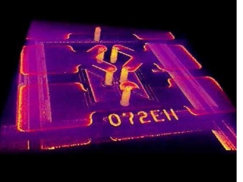
- Engineering and modeling: Test structure design, multi-physics FEA, Computation Fluid Dynamics, magnetics, high-frequency analysis, Spice simulations
- Ansys full physics modeling software package
- HFSS
Featured E-book
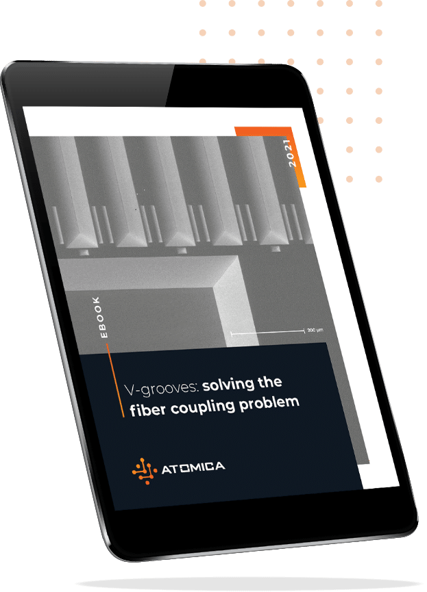
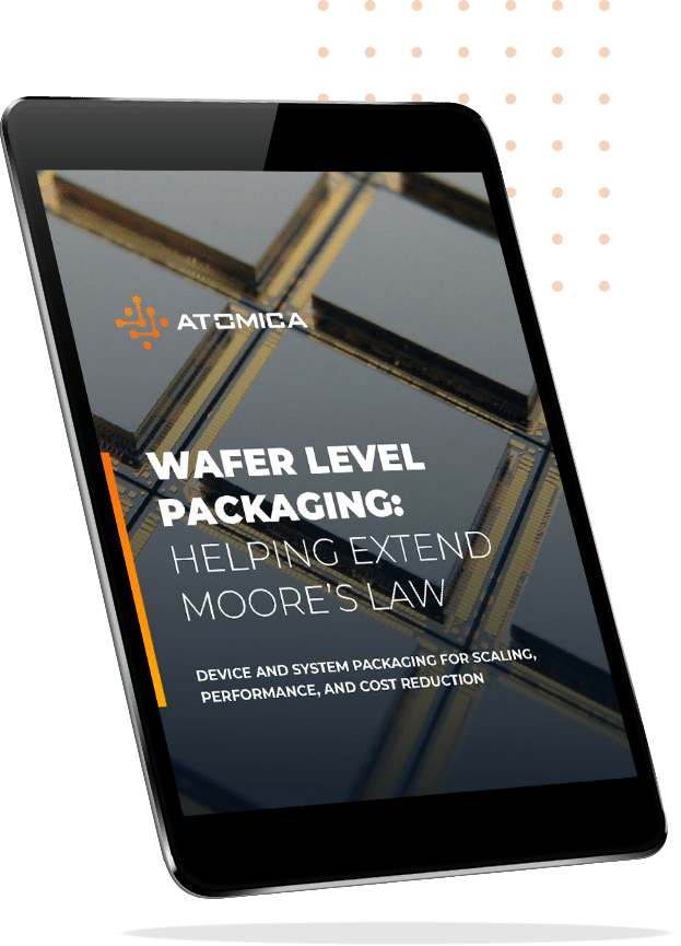
Discover more about WLP, one of the great enablers of 3-D integration
Featured E-book
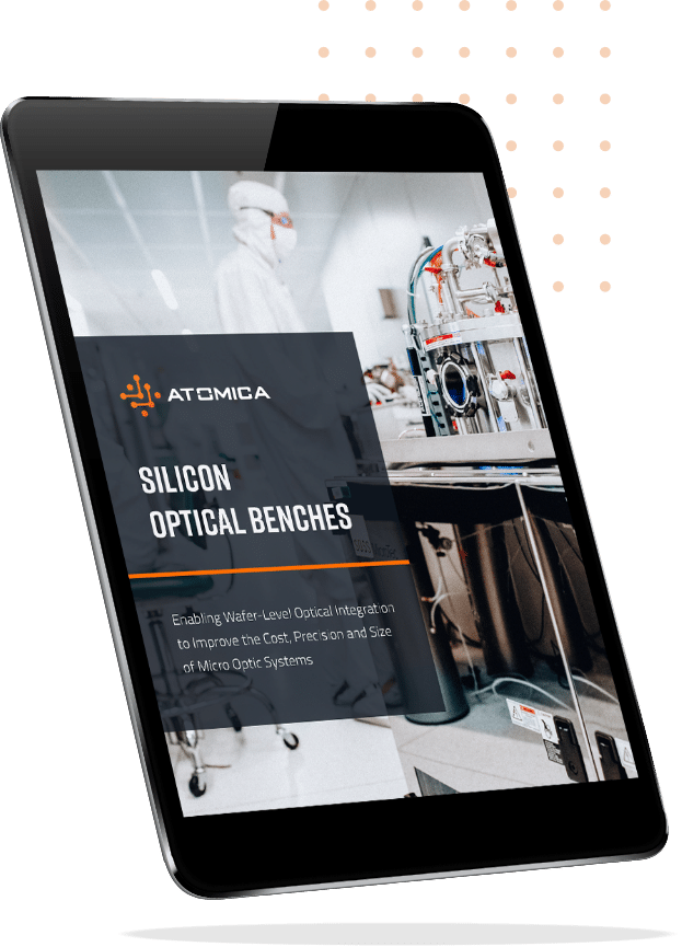
Learn how SiOBs enable micro level optical integration, thus improving cost, precision and reducing size.

Featured E-book
Learn about the power of 3D lithography (greyscale) to create complex works, like the Mona Lisa, at the wafer level.
Featured E-book
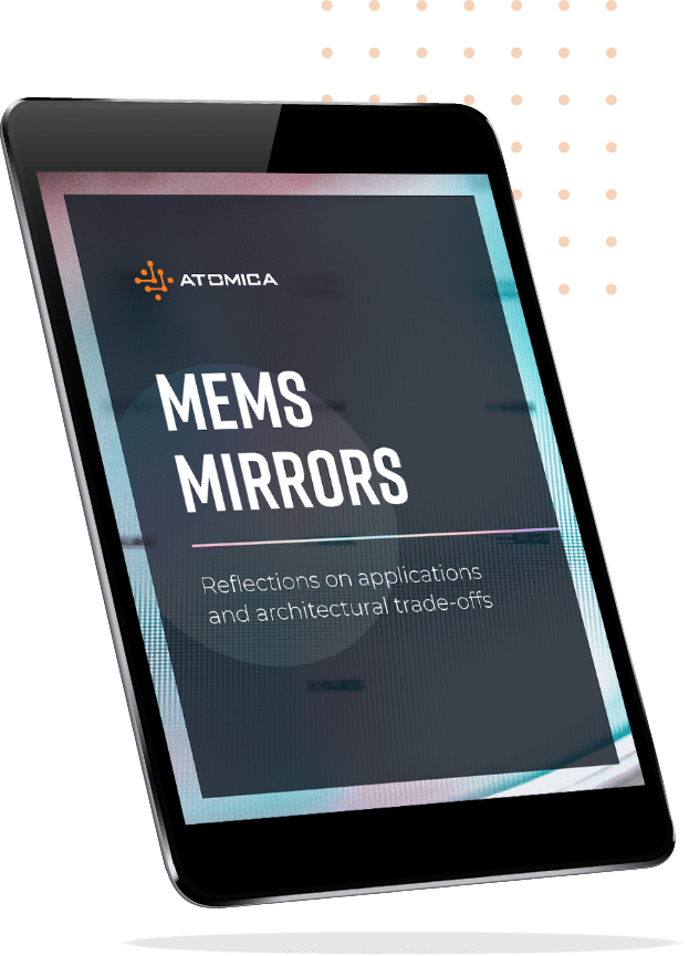
Managing the six key design decisions in the creation of MEMS Mirrors
Why Atomica?
-
Largest US MEMS Foundry
Atomica serves its customers from a 13-acre, 130,000 ft2 manufacturing campus (including a 30,000 ft2 class 100 cleanroom) in Santa Barbara, California. We operate over 400 sophisticated 150mm and 200mm tools and are ISO 9001 and ITAR certified. This makes us the largest independent MEMS fab in the United States, well-positioned to support the growing demand for domestic production of critical sensors, photonics, and biochips.
-
Unique collaborative methodology to ensure program success
At Atomica, we are resolved to help our customers bring their innovations to life using our proven phase-gate process to successfully navigate the challenges of design, development, prototype, scale-up, and high-volume production. Our multi-disciplinary team of scientists and manufacturing engineers tackles the hardest process development and integration challenges with an eye toward manufacturability (DFM). Our methodology entails rigorous project management to optimize resources, mitigate risks, and deliver predictable results.
-
Extraordinary engineering expertise
Atomica has over 20 years of experience commercializing technologies that change the future. Our extensive experience spans the full spectrum of MEMS, including photonics, sensors, microfluidic biochips, and other micro components. We have over 20 Phds on-site and we’ve worked on hundreds of programs to date. You could say we’ve seen it all. This experience combined with our volume production facility help ensure customers get to market fast with the highest chance of commercial success.
-
Exceptional flexibility in materials and project types
Atomica has a versatile and flexible engagement model. We are able to engage using our standard processes or provide bespoke, custom process development. We will consider programs of many sizes, as long as they hold promise to have an impact on the world once they reach production. Atomica also is able to handle a very broad range of materials providing access to an extensive set of processes and materials unavailable in CMOS fabs, including noble metals, polymers, and virtually any substrate (e.g., silicon, SOI, glass, fused silica, quartz, borosilicate, piezos, and III-V).