Wafer-level integration for 3D Sensing and LiDAR
Light engines are now being used to create 3D maps enabling computers to see. Silicon Optical Benches (SiOBs) integrate the various light sources, mirrors, photodetectors, or diffractive optical elements to miniaturize such systems. The following eBook explains how SiOBs enable wafer-level optical integration, thus improving the cost, precision, and size of micro optic systems.
Get your eBook

SiOBs are a wafer-level platform, that efficiently integrate the many discrete elements of an optical system, including lasers, lenses, mirrors, photodetectors, filters, isolators, rotators, and couplers.
What is a Silicon Optical Bench?
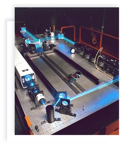
SiOBs are named after the benchtop apparatus, optical benches used by scientists to study light phenomena for more than a century. The concept of a SiOB is the same, except they use silicon with discrete optical elements such as lenses, lasers, mirrors, or beam splitters placed into kinematic cavities or pits in the silicon designed to precisely hold each element in the correct X,Y, and Z position.
Benefits of a Silicon Optical Bench
Shrinking an optical bench down onto silicon affords many benefits over alternative optical assembly approaches.
01. SIZE
Optical elements can be packed onto chips with sub-micron precision and density. The results are optical “engines”, sensors, and transceivers that are a fraction of the size of conventionally assembled optical systems.
02. Cost
The economies of scale and thus cost savings afforded by wafer level manufacturing are considerable. Wafer processes enable automated test and inspection, thus further reducing cost compared to serial testing approaches.
03. PRECISION
Lithographic precision of features combined with the latest advances in placement technology ensure that optical elements are placed within very tight tolerances, thus enabling high fidelity in the manufacturing of optical systems.
04. LOW LOSS
SiOBs can be engineered for low loss by leveraging free-space optical paths or coupling to low loss waveguides.
05. HERMETICITY
SiOBs are commonly topped with a lid wafer using wafer-level bonding techniques allowing for the creation of hermetic cavities for the entire optical system. This ensures high reliability and lifetime protection from environmental hazards such as moisture, oxygen and dust which can degrade the performance of many optical elements.
SiOB Manufacturing Considerations
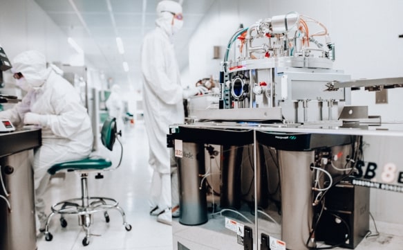
The design and manufacture of SiOBs requires a complex set of technologies and process capabilities. This brings together disciplines not commonly found under one roof. Anyone considering the use of SiOBs would be well served to consider the variables and processes discussed in the following eBook to ensure the right partners to field a successful product.
LEARN MORE
DOWNLOADING OUR EBOOK
"Silicon Optical Benches" - Enabling Wafer-Level Optical Integration to Improve the Cost, Precision, and Size of Micro Optic Systems